


GaN semiconductor centre boosts Singapore’s chip leadership
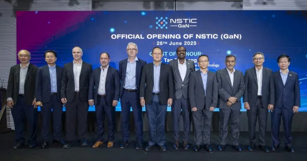
Singapore has officially launched the National Semiconductor Technology Innovation Centre (NSTIC) for gallium nitride (GaN) semiconductors, marking a key milestone in its bid to lead in advanced chip development. Created through partnerships with A*STAR, DSO National Laboratories, and Nanyang Technological University (NTU), the centre aims to accelerate innovation in high-frequency chip applications such as 5G/6G, satellite communications, and radar systems.
The facility is positioned to drive faster research, prototyping, and commercialization. It also enhances Singapore’s role as a hub for compound semiconductor growth across Asia.
Laying the foundation for next-gen semiconductors
The NSTIC is a strategic outcome of Singapore’s Semiconductor Vision Statement 2030, a national roadmap designed to deepen local expertise in compound semiconductors, advanced packaging, and next-generation materials. Gallium nitride, known for its high thermal conductivity and energy efficiency, is a standout material in the push beyond traditional silicon.
Unlike silicon chips, GaN devices operate at higher voltages, withstand extreme temperatures, and are ideal for compact, high-power systems. These properties make GaN crucial for defense, aerospace, and next-generation telecommunications.
The new NSTIC facility consolidates key infrastructure in one location. It includes wafer fabrication tools, device characterization labs, and pilot-scale production capabilities. This enables researchers and engineers to design, test, and scale GaN chips without relying on fragmented workflows or overseas fabs.
The project is led by A*STAR’s Institute of Microelectronics (IME), with support from global and regional partners. These collaborators can access the centre to co-develop solutions or validate prototypes for commercial deployment.
Partner-led innovation and industry access
NSTIC’s strength lies in its integration of research, industry, and education. By working alongside DSO and NTU, the centre supports both national security goals and private-sector R&D. Local firms now have access to shared infrastructure that shortens development cycles and reduces reliance on foreign manufacturing.
According to A*STAR, the centre’s role is to serve as a bridge between academic research and industrial scale-up. Startups, SMEs, and multinational corporations can all leverage the platform. This model supports Singapore’s Economic Development Board (EDB) goal to double the semiconductor sector’s output by 2030.
The government has emphasized that innovation ecosystems like NSTIC are not just research centres—they are key enablers for commercialization. By providing ready access to equipment, expertise, and strategic networks, NSTIC will help local firms move from idea to market with greater speed and efficiency.
Why GaN matters for Asia’s chip future
Gallium nitride is not simply a next-gen material—it is a strategic differentiator. As restrictions tighten around high-performance silicon chips, especially in geopolitically sensitive sectors, countries like Singapore are looking to GaN to fill the performance and supply chain gaps.
GaN’s ability to support power-efficient and high-frequency operations makes it ideal for emerging needs in defense electronics, EV charging, and space systems. This shift reflects a broader trend in Asia, where nations are investing in resilient, localized semiconductor ecosystems.
Singapore’s NSTIC complements wider regional investments, including Taiwan’s Hsinchu expansions and Japan’s compound foundry partnerships. Together, these projects signal Asia’s shift toward next-generation chip sovereignty—driven by new materials, smarter infrastructure, and collaborative research hubs.
From national project to regional export hub
NSTIC is expected to evolve into a regional innovation hub for compound semiconductors. Early-stage efforts will focus on smart mobility, radar systems, power converters, and AI-integrated chip platforms. These are all industries where GaN shows significant promise.
In the future, NSTIC could expand its portfolio to include materials like gallium oxide and silicon carbide (SiC), both known for their wide bandgap advantages. This would allow Singapore to lead not only in chip design but also in material science innovation.
The global GaN market is projected to exceed $5 billion by 2028, and Singapore’s early investment places it in a strong commercial position. By becoming a first mover in this space, the country increases its competitiveness while supporting economic resilience in the region.
Singapore sets the pace in GaN innovation
With the launch of NSTIC’s GaN semiconductor centre, Singapore is advancing its role as a key player in Asia’s semiconductor future. By uniting research institutions, government support, and industrial collaboration, it is setting a new benchmark for compound chip innovation.
As global demand rises and material science reshapes the semiconductor sector, Singapore’s focus on GaN technologies offers not just strategic value—but also long-term leadership in high-frequency electronics.