


South Korean chipmaker advances next-gen memory for AI and high-performance computing
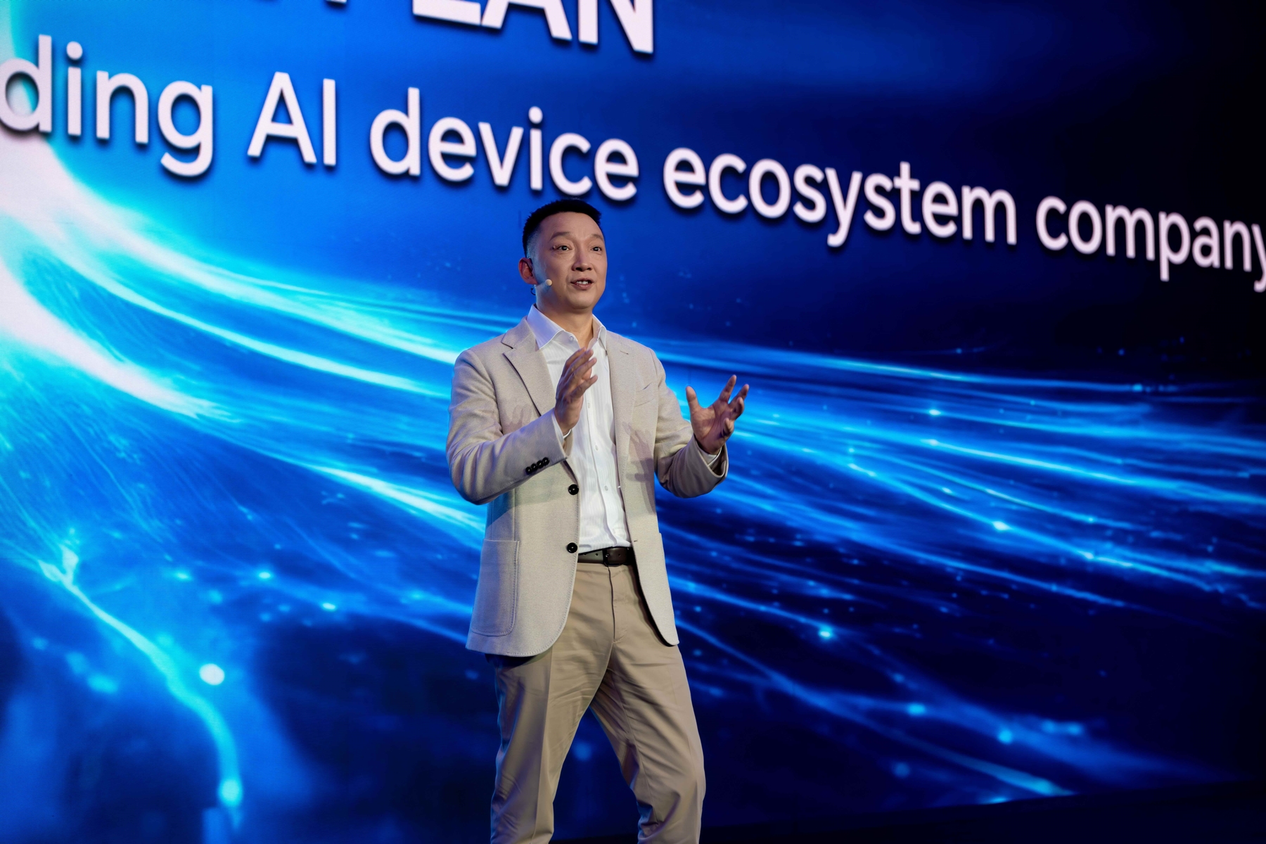
SK Hynix, South Korea’s second-largest semiconductor manufacturer, has revealed the world’s first 3D-stacked DRAM prototype, marking a major innovation in memory architecture. The announcement, made on June 10, 2025, positions SK Hynix at the forefront of global competition in next-generation memory solutions for artificial intelligence (AI) and high-performance computing (HPC).
Pushing memory boundaries in the AI era
SK Hynix, a key supplier to global tech giants including Nvidia and Microsoft, has long specialized in dynamic random-access memory (DRAM) and NAND flash. As demand for AI accelerators and data-centric computing grows, conventional DRAM is reaching physical and performance limits.
Traditional DRAM structures rely on planar stacking, which limits bandwidth and energy efficiency. The transition to a vertically stacked 3D structure represents a paradigm shift—akin to the earlier revolution in 3D NAND—that can overcome bottlenecks in density, latency, and thermal management.
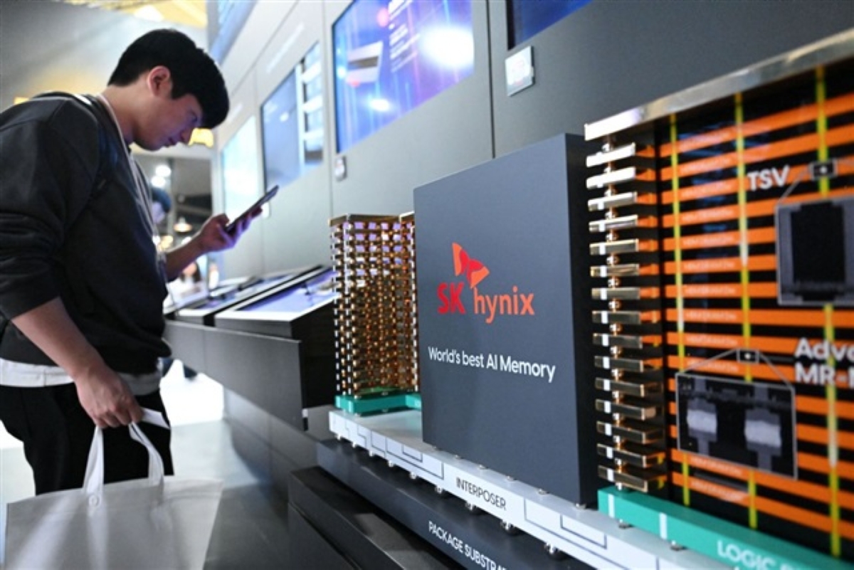
SK Hynix’s 3D DRAM design stacks multiple layers of memory cells vertically, using through-silicon via (TSV) technology and proprietary bonding techniques. The prototype uses five layers and is designed to scale beyond 16 layers in future commercial models.
Innovation meets global demand
According to SK Hynix, this 3D DRAM will initially target AI workloads, including training large language models and powering data centers handling real-time inference. The company is collaborating with global hyperscalers and chipmakers to customize performance for next-gen GPUs and custom AI processors.
The prototype was developed at SK Hynix’s Icheon R&D campus and will enter pilot production in 2026. Analysts believe the company’s early lead could help it secure strategic partnerships in the AI supply chain, particularly as countries prioritize domestic semiconductor capabilities.
SK Hynix is also leveraging government incentives under South Korea’s national K-Chips Act to support advanced packaging and memory innovation. Its roadmap includes extending 3D DRAM to mobile devices and automotive chips by 2027.
South Korea’s edge in memory leadership
This development reinforces South Korea’s global leadership in memory semiconductors. While Taiwan dominates logic chip manufacturing via TSMC, South Korea’s SK Hynix and Samsung are leading the charge in advanced memory.
With AI workloads ballooning, memory architectures are becoming critical bottlenecks. SK Hynix’s 3D DRAM could be a game-changer—enabling faster model training, greater power efficiency, and better space optimization in dense data centers.
It also arrives amid increasing U.S.–China tech tensions, with AI infrastructure emerging as a proxy battleground. By unveiling this breakthrough, SK Hynix strengthens its geopolitical and commercial positioning as a neutral and technologically superior memory provider.
Commercialization and strategic adoption
SK Hynix aims to move from prototype to mass production within 18 months, with initial deployment in AI clusters and supercomputers. As memory demand grows exponentially—projected to surpass 1,000 exabytes annually by 2027—the commercial stakes are high.
Potential collaborations with OpenAI, Meta, and regional cloud providers in Japan and Singapore are under review. Analysts expect the technology to eventually migrate into consumer applications such as AR/VR headsets and AI-native smartphones.
SK Hynix’s focus on scaling 3D DRAM aligns with broader industry trends toward chiplet-based architectures and heterogeneous integration. If successful, it could help redefine the next decade of AI memory standards.
A stacked leap forward in semiconductor design
The debut of SK Hynix’s 3D DRAM prototype marks a historic moment for the global memory industry. By unlocking vertical scaling, SK Hynix is offering a tangible solution to one of AI’s biggest infrastructure constraints.
As competition heats up between AI hardware giants, innovations like 3D-stacked memory will play a pivotal role in shaping performance, sustainability, and global technology leadership. South Korea, through SK Hynix, is making clear that it intends to stay ahead in that race.